Scanning Probe Microscopy Studies of Self-Assembled Nanostructures
Scanning Probe Microscopy Studies of Self-Assembled Nanostructures
Sangyeob Lee
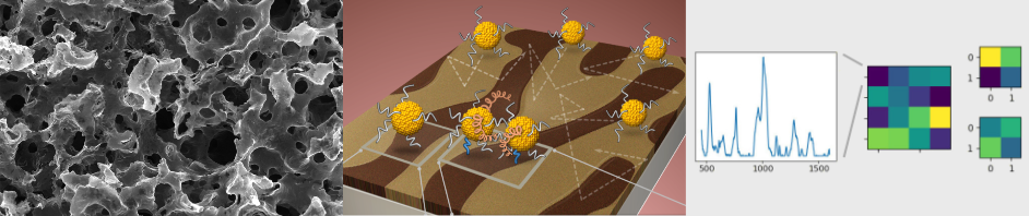
Metallic nanostructures have various promising applications. For example, gold nanoclusters of diameter approximately 3 nm exhibit excellent catalytic activity, even though bulk gold is catalytically inert. Metallic nanostructures may also be utilized for nanoscale electronics and sensors. In order to realize these applications, it is crucial to study the electronic properties of these nanostructures, which often differ significantly from those of bulk materials.
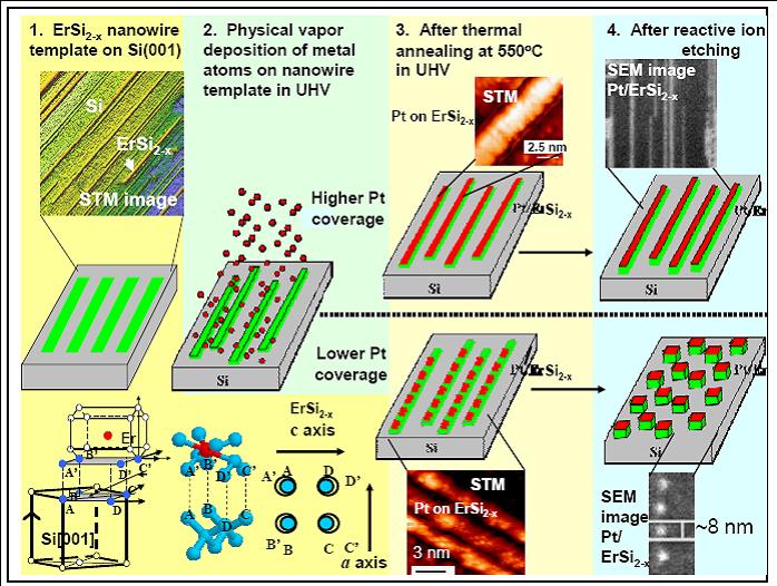
Our group uses a unique silicon-compatible fabrication process for ordered noble metal nanostructures. On silicon, we fabricate self-assembled rare earth metal nanowires, such as dysprosium disilicide (DySi2) and erbium disilicide (ErSi2), which are then used as templates for noble metal nanostructures. As shown in the figure below, evaporated nobel metal particles (gold or platinum) aggregate preferentially on top of these nanowire templates, forming an ordered array of noble metal nanoclusters or nanowires depending on coverage.
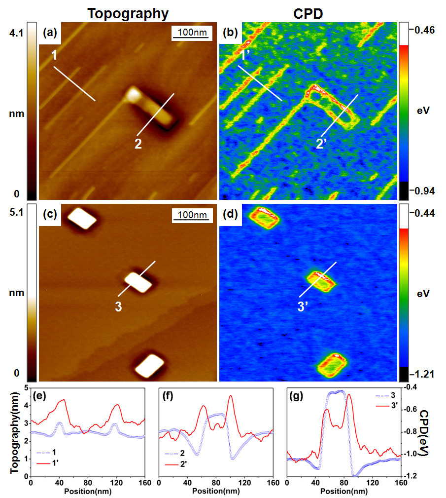
We use an ultrahigh vacuum (UHV) system maintained at 10-11 torr to fabricate and characterize nanostructures in a contaminant-free environment. This UHV system houses a scanning tunneling microscope (STM) and Kelvin probe force microscope (KPFM). The STM produces atomic-resolution images of surfaces and has a scanning tunneling spectroscopy (STS) function that elucidates the density of states and electronic transport properties of nanostructures. The KPFM, which is a modification of the atomic force microscope (AFM), simultaneously measures the nanoscale topography and electronic work function profiles of nanostructures. It is possible to attain atomic lateral resolution with the UHV KPFM, and the resolution of work function measurement is about 10 meV. The KPFM images below show local topography (left) and contact potential difference* (right) of DySi2 nanowires and a DySi2 nanoisland.
* The contact potential difference is the difference between the electronic work functions of the sample and KPFM probe.